Jump to: Journal Articles, Conference Publications, Conference Presentations, Books, Patents

Journal Articles

  1. Advancements in 300 mm GaN-on-Si Technology With Industry’s First Circuit Demonstration of Monolithically Integrated GaN and Si Transistors
    Q. Yu, A.A. Farid, I. Momson, J. Garrett, H. Vora, S. Bader, A. Zubair, P. Koirala, M. Beumer, A. Vyatskikh, P. Nordeen, T. Hoff, M. Radosavljevic, S. Rami, F. O’Mahony, H.W. Then,
    IEEE Microwave and Wireless Technology Letters (), 1-4 (2024).
  2. Enhancement-Mode 300-mm GaN-on-Si(111) With Integrated Si CMOS for Future mm-Wave RF Applications
    H.W. Then, M. Radosavljevic, Q. Yu, A. Latorre-Rey, H. Vora, S. Bader, I. Momson, D. Thomson, M. Beumer, P. Koirala, J. Peck, A. Oni, T. Hoff, R. Jordan, T. Michaelos, N. Nair, P. Nordeen, A. Vyatskikh, I. Ban, A. Zubair, S. Rami, P. Fischer,
    IEEE Microwave and Wireless Technology Letters 33(6), 835-838 (2023).
  3. Electric Fields and Surface Fermi Level in Undoped GaN/AlN Two-Dimensional Hole Gas Heterostructures
    Ł. Janicki, R. Chaudhuri, S.J. Bader, H.G. Xing, D. Jena, R. Kudrawiec,
    physica status solidi (RRL) – Rapid Research Letters 15(4), 2000573 (2021).
  4. Next generation electronics on the ultrawide-bandgap aluminum nitride platform
    A.L. Hickman, R. Chaudhuri, S.J. Bader, K. Nomoto, L. Li, J.C.M. Hwang, H.G. Xing, D. Jena,
    Semiconductor Science and Technology 36(4), 044001 (2021).

      ★ Invited Paper
  5. First RF Power Operation of AlN/GaN/AlN HEMTs With >3 A/mm and 3 W/mm at 10 GHz
    A. Hickman, R. Chaudhuri, L. Li, K. Nomoto, S.J. Bader, J.C.M. Hwang, H.G. Xing, D. Jena,
    IEEE Journal of the Electron Devices Society 9(), 121-124 (2021).
  6. Prospects for Wide bandgap and Ultrawide bandgap CMOS Devices
    S.J. Bader, H. Lee, N. Chowdhury, R. Chaudhuri, S. Huang, A. Hickman, H.W. Then, A. Molnar, T. Palacios, H.G. Xing, D. Jena,
    IEEE Transactions on Electron Devices 67, 4010-4020 (2020).

      ★ Invited Paper
  7. GaN HEMTs on Si with Regrown Contacts and Cutoff/Maximum Oscillation Frequencies of 250/204 GHz
    L. Li, K. Nomoto, M. Pan, W. Li, A. Hickman, J. Miller, K. Lee, Z. Hu, S.J. Bader, S.M. Lee, J.C. Hwang, D. Jena, H.G. Xing,
    IEEE Electron Device Letters 41, 689-692 (2020).
  8. Molecular Beam Epitaxy Growth of Large-Area GaN/AlN 2D Hole Gas Heterostructures
    R. Chaudhuri, S.J. Bader, Z. Chen, D. Muller, H.G. Xing, D. Jena,
    physica status solidi (b) , 1900567 (2020).
  9. High Breakdown Voltage in RF AlN/GaN/AlN Quantum Well HEMTs
    A. Hickman, R. Chaudhuri, S.J. Bader, K. Nomoto, K. Lee, H.G. Xing, D. Jena,
    IEEE Electron Device Letters 40(8), 1293-1296 (2019).

  10. Wurtzite Phonons and the Mobility of a GaN / AlN 2D Hole Gas
    S.J. Bader, R. Chaudhuri, M.F. Schubert, H.W. Then, H.G. Xing, D. Jena,
    Applied Physics Letters 114(253501), 1-5 (2019).

      ★ Editor’s Pick
  11. A polarization-induced 2D hole gas in undoped gallium nitride quantum wells
    R. Chaudhuri, S.J. Bader, Z. Chen, D.A. Muller, H. Xing, D. Jena,
    Science 365(6460), 1454-1457 (2019).

  12. Gate-recessed E-mode p-channel HFET with high on-current based on GaN/AlN 2D hole gas
    S.J. Bader, R. Chaudhuri, K. Nomoto, A. Hickman, Z. Chen, H.W. Then, D.A. Muller, H.G. Xing, D. Jena,
    IEEE Electron Device Letters 39(12), 1848-1851 (2018).

  13. A New Holistic Model of 2-D Semiconductor FETs
    E.G. Marin, S.J. Bader, D. Jena,
    IEEE Transactions on Electron Devices 65(3), 1239-1245 (2018).
  14. Terahertz spectroscopy of an electron-hole bilayer system in AlN/GaN/AlN quantum wells
    H.C. Quispe, S.M. Islam, S. Bader, A. Chanana, K. Lee, R. Chaudhuri, A. Nahata, H.G. Xing, D. Jena, B. Sensale-Rodriguez,
    Applied Physics Letters 111(7), 073102 (2017).
  15. High breakdown single-crystal GaN p-n diodes by molecular beam epitaxy
    M. Qi, K. Nomoto, M. Zhu, Z. Hu, Y. Zhao, V. Protasenko, B. Song, X. Yan, G. Li, J. Verma, S. Bader, P. Fay, H.G. Xing, D. Jena,
    Applied Physics Letters 107(23), 232101 (2015).

  16. Coherence and decay of higher energy levels of a superconducting transmon qubit
    M.J. Peterer, S.J. Bader, X. Jin, F. Yan, A. Kamal, T.J. Gudmundsen, P.J. Leek, T.P. Orlando, W.D. Oliver, S. Gustavsson,
    Physical Review Letters 114(1), 010501 (2015).
  17. Effective incidence angles of sky-diffuse and ground-reflected irradiance for various incidence angle modifier types
    E. Strobach, D. Faiman, S.J. Bader, S.J. Hile,
    Solar Energy 89, 81-88 (2013).

Conference Publications

  1. DrGaN: an Integrated CMOS Driver-GaN Power Switch Technology on 300mm GaN-on-Si with E-mode GaN MOSHEMT and 3D Monolithic Si PMOS
    H.W. Then, M. Radosavljevic, S. Bader, A. Zubair, H. Vora, N. Nair, P. Koirala, M. Beumer, P. Nordeen, A. Vyatskikh, T. Hoff, J. Peck, R. Nahm, T. Michaelos, E. Khora, R. Jordan, C. Hoffman, N. Franco, A. Oni, S. Beach, D. Garg, D. Frolov, A. Latorre-Rey, A. Mitaenko, J. Rangaswamy, S. Sarkar, S. Ahmed, V. Rayappa, H. Chiu, A. Hubert, S. Brophy, N. Arefm, N. Desai, H. Krishnamurthy, J. Yu, K. Ravichandran, P. Fischer,
    2023 International Electron Devices Meeting (IEDM) (2023).
  2. Scaled Submicron Field-Plated Enhancement Mode High-K Gallium Nitride Transistors on 300mm Si(111) Wafer with Power FoM (RON xQGG) of 3.1 mohm-nC at 40V and fT/fMAX of 130/680GHz
    H.W. Then, M. Radosavljevic, P. Koirala, M. Beumer, S. Bader, A. Zubair, T. Hoff, R. Jordan, T. Michaelos, J. Peck, I. Ban, N. Nair, H. Vora, K. Joshi, I. Meric, A. Oni, N. Desai, H. Krishnamurthy, K. Ravichandran, J. Yu, S. Beach, D. Frolov, A. Hubert, A. Latorre-Rey, S. Rami, J. Rangaswamy, Q. Yu, P. Fischer,
    2022 International Electron Devices Meeting (IEDM) (2022).
  3. A Fully Integrated 3.2-4.7GHz Doherty Power Amplifier in 300mm GaN-on-Si Technology
    Q. Yu, D. Thomson, H.W. Then, A. Latorre-Rey, M. Radosavljevic, M. Beumer, P. Koirala, N. Thomas, N. Nair, H. Vora, S. Bader, S. Rami,
    2022 IEEE BiCMOS and Compound Semiconductor Integrated Circuits and Technology Symposium (BCICTS) (2022).
  4. 5G mmWave Power Amplifier and Low-Noise Amplifier in 300mm GaN-on-Si Technology
    Q. Yu, H.W. Then, D. Thomson, J. Chou, J. Garrett, I. Huang, I. Momson, S. Ravikumar, S. Hwangbo, A. Latorre-Rey, A. Roy, M. Radosavljevic, M. Beumer, P. Koirala, N. Thomas, N. Nair, H. Vora, S. Bader, J. Rode, J. Jensen, S. Rami,
    2022 IEEE Symposium on VLSI Technology and Circuits (VLSI Technology and Circuits) (2022).
  5. Advanced Scaling of Enhancement Mode High-K Gallium Nitride-on-300mm-Si(111) Transistor and 3D Layer Transfer GaN-Silicon Finfet CMOS Integration
    H.W. Then, M. Radosavljevic, P. Koirala, N. Thomas, N. Nair, I. Ban, T. Talukdar, P. Nordeen, S. Ghosh, S. Bader, T. Hoff, T. Michaelos, R. Nahm, M. Beumer, N. Desai, P. Wallace, V. Hadagali, H. Vora, A. Oni, X. Weng, K. Joshi, I. Meric, C. Nieva, S. Rami, P. Fischer,
    International Electron Devices Meeting (2021).
  6. GaN/AlN p-channel HFETs with Imax > 420mA/mm and 20 GHz fT/fMAX
    K. Nomoto, R. Chaudhuri, S.J. Bader, L. Li, A. Hickman, S. Huang, H. Lee, T. Maeda, H.W. Then, M. Radosavljevic, P. Fischer, A. Molnar, J.C.M. Hwang, H.G. Xing, D. Jena,
    International Electron Devices Meeting (2020).
  7. GaN/AlN Schottky-gate p-channel HFETs with InGaN contacts and 100 mA/mm on-current
    S.J. Bader, R. Chaudhuri, A. Hickman, K. Nomoto, S. Bharadwaj, H.W. Then, H.G. Xing, D. Jena,
    International Electron Devices Meeting (2019).
  8. Wide-bandgap Gallium Nitride p-channel MISFETs with enhanced performance at high temperature
    K. Nomoto, S.J. Bader, K. Lee, S. Bharadwaj, Z. Hu, H.G. Xing, D. Jena,
    Device Research Conference – Conference Digest, DRC (2017).
  9. S-shaped negative differential resistance in III-Nitride blue quantum-well laser diodes grown by plasma-assisted MBE
    H. Turski, R. Yan, S.J. Bader, G. Muziol, C. Skierbiszewski, H.G. Xing, D. Jena,
    Device Research Conference – Conference Digest, DRC (2017).
  10. Introducing the spiked p-n junction for tunnel devices and current gain
    S.J. Bader, D. Jena,
    Device Research Conference – Conference Digest, DRC (2016).
  11. CPV Vs. PV from a grid-matching perspective
    E. Strobach, S. Bader, D. Faiman, A.A. Solomon, G. Meron,
    AIP Conference Proceedings (2012).

Conference Presentations

  1. GaN MOSHEMT Transistor Technology and Integrated ESD Device Solutions on 300mm GaN-on-Si(111) wafers
    H.W. Then, H. Gossner, S.J. Bader, M. Radosavljevic, R. Geiger, L. Giles, P. Koirala, M. Beumer, H. Vora, N. Nair, P. Nordeen, A. Vyatskikh, T. Hoff, J. Peck, T. Michaelos, E. Khora, R. Jordan, R. Nahm, A. Zubair, P. Fischer,
    EOS/ESD Symposium 2023 (2023).
  2. 3D heterogeneous integration of GaN and Si transistor channels by Layer Transfer for Energy-Efficient and Compact System-on-Chip
    A. Zubair, H.W. Then, M. Radosavljevic, I. Ban, P. Koirala, M. Beumer, S.J. Bader, H. Vora, N. Nair, T. Michaelos, J. Peck, T. Hoff, P. Nordeen, A. Vyatskikh, P. Fischer,
    Materials Research Society Spring Meeting (2023).
  3. CMP Opportunities for Emerging Semiconductor Technologies
    T. Hoff, H.W. Then, M. Radosavljevic, P. Nordeen, A. Vyatskikh, P. Koirala, M. Beumer, S.J. Bader, A. Zubair, T. Michaelos, J. Peck, N. Nair, H. Vora, A. Wagner, R. Nahm, D. Kohen, R. Vreeland, W. Brezinski, P. Fischer,
    Center for Advanced Materials Processing CMP Symposium (2023).
  4. Progress in CMOS Integration in Wide-bandgap Electronics
    S.J. Bader,
    International Conference on Solid State Devices and Materials (2021).

      ★ Invited Speaker
  5. Fully passivated InAlN/GaN HEMTs on silicon with fT/fMAX of 144/141 GHz
    K. Nomoto, M. Pan, Z. Hu, J. Miller, W. Li, A. Hickman, K. Lee, S.J. Bader, S.M. Lee, D. Jena, H.G. Xing,
    Topical Workshop on Heterostructure Microelectronics (2019).
  6. The Mobility of a GaN-on-AlN Two-Dimensional Hole Gas
    S.J. Bader, R. Chaudhuri, G. Xing, D. Jena,
    International Conference on Nitride Semiconductors (2019).
  7. 2D Electron-Hole Gas Bilayers in Undoped AlN/GaN/AlN
    R. Chaudhuri, J. Miller, S.J. Bader, G. Xing, D. Jena,
    International Conference on Nitride Semiconductors (2019).
  8. Record Small-Signal RF and Off-State Breakdown Characteristics in AlN\/
    GaN\/AlN HEMTs

    A.L. Hickman, R. Chaudhuri, S.J. Bader, K. Nomoto, D. Jena, G. Xing,
    International Conference on Nitride Semiconductors (2019).
  9. Contactless Electroreflectance Studies of the Surface Fermi Level in GaN/
    AlN Heterostructures with Buried 2D Hole Gas

    L. Janicki, R. Chaudhuri, S.J. Bader, G. Xing, D. Jena, R. Kudrawiec,
    International Conference on Nitride Semiconductors (2019).
  10. GaN-on-AlN as a Superior Platform for Integrated Wide-bandgap Electronics
    S.J. Bader, A. Hickman, R. Chaudhuri, K. Nomoto, H.W. Then, H.G. Xing, D. Jena,
    Government Microcircuit Applications and Critical Technology Conference (2019).
  11. The GaN-on-AlN Platform for Integrated Wide-bandgap Electronics
    S.J. Bader, A. Hickman, R. Chaudhuri, K. Nomoto, H.G. Xing, D. Jena,
    SRC Student Poster at IEEE International Electron Devices Meeting (2018).
  12. Enhancement-mode GaN-on-AlN p-channel HFETs with record on-current
    S.J. Bader, R. Chaudhuri, S. Bharadwaj, A. Hickman, K. Nomoto, H.W. Then, H.G. Xing, D. Jena,
    International Workshop on Nitrides (2018).
  13. Polarization-induced 2D Hole Gas in Undoped GaN/AlN Heterostructures
    R. Chaudhuri, S. Bader, Z. Chen, D. Muller, H. Xing, D. Jena,
    International Workshop on Nitrides (2018).
  14. First RF Strained AlN/GaN/AlN Quantum Well HEMTs on 6H-SiC
    A. Hickman, S.J. Bader, R. Chaudhuri, K. Nomoto, S. Islam, H.G. Xing, D. Jena,
    International Workshop on Nitrides (2018).
  15. 2D Hole Gas in MBE grown GaN/AlN Heterostructures
    R. Chaudhuri, S. Bader, A. Hickman, R. Page, H. Xing, D. Jena,
    Electronic Materials Conference (2018).
  16. High-Voltage Properties of Strained GaN Quantum Well HEMTs on AlN
    A. Hickman, S.J. Bader, R. Chaudhuri, K. Nomoto, S. Islam, H.G. Xing, D. Jena,
    Compound Semiconductor Week (2018).
  17. Molecular Beam Epitaxy of High Mobility AlN/GaN/AlN Quantum Well FET Structures on 6H-SiC
    R. Chaudhuri, S. Bader, A. Hickman, S. Islam, H.G. Xing, D. Jena,
    International Workshop on the Physics of Semiconductor Devices (2017).
  18. GaN/AlN Quantum Well FETs on AlN/SiC Platform Using High Temperature MBE Growth
    R. Chaudhuri, S. Islam, S. Bader, A.L. Hickman, S. Bharadwaj, H.G. Xing, D. Jena,
    Electronic Materials Conference (2017).

Books/Chapters

  1. Linearity Aspects of High Power Amplification in GaN Transistors
    S.J. Bader, K. Shinohara, A. Molnar,
    in High-frequency GaN Electronic Devices, published by Springer (2020).

Patents

  1. “Gallium Nitride (GaN) integrated circuit technology”
    N.K. Thomas, S.J. Bader, M. Radosavljevic, H.W. Then, P. Koirala, N. Nair,
    Pending (17/402054), submitted 2023.
  2. “Gallium Nitride (GaN) layer transfer and regrowth for integrated circuit technology”
    P. Koirala, S. Ghosh, P. Nordeen, T. Talukdar, T. Hoff, I. Ban, K. Jun, S.J. Bader, M. Radosavljevic, N.K. Thomas, P.B. Fischer, H.W. Then,
    Pending (17/408025), submitted 2023.
  3. “Gallium Nitride (GaN) integrated circuit technology with multi-layer epitaxy and layer transfer”
    S. Ghosh, H.W. Then, P. Koirala, T. Talukdar, P. Nordeen, N. Nair, M. Radosavljevic, I. Ban, K. Jun, J. Gupta, P.B. Fischer, N.K. Thomas, T. Hoff, S.J. Bader,
    Pending (17/410257), submitted 2023.
  4. “Gallium Nitride (GaN) selective epitaxial windows for integrated circuit technology”
    S.J. Bader, P. Koirala, N.K. Thomas, H.W. Then, M. Radosavljevic,
    Pending (17/458097), submitted 2023.
  5. “Gallium nitride (gan) transistors with lateral drain depletion”
    H.W. Then, M. Radosavljevic, S.J. Bader, P. Koirala, M.S. Beumer, H.C. Vora, A. Zubair,
    Pending (US20240021725A1), submitted 2022.
  6. RF high-electron-mobility transistors including group III-N stress neutral barrier layers with high breakdown voltages
    A. Hickman, R. Chaudhuri, S.J. Bader, D. Jena, H.G. Xing,
    Granted (US11710785B2), 2023.
  7. A high-voltage p-channel FET based on III-Nitride heterostructures
    S.J. Bader, R. Chaudhuri, D. Jena, H.G. Xing,
    Granted (US11522080B2), 2022.
  8. Polarization-induced 2D hole gases for high-voltage p-channel transistors
    R. Chaudhuri, S.J. Bader, D. Jena, H.G. Xing,
    Granted (US011158709B2), 2021.

Misc helpful undergraduate content

Term Papers

Applied Superconductivity:
The Transmon Qubit

Electrical, Optical & Magnetic Materials/Devices:
Bulk-heterojunction Organic Photovoltaics

Quantum Mechanics III:
Intro to Quantum Error Correction

Atomic and Optical Physics I:
Quantum Non-demolition Photon Detection
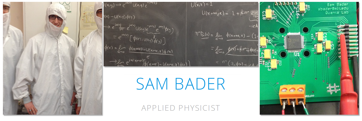
Summer Projects

Quanta Lab:
Manual for Laser Stabilization

Institute for Quantum Computing:
Holevo Additivity Violation Search

Ben Gurion Solar Energy Center:
Power-grid Interactions Notes

Miscellaneous notes

Lie Algebras and Representation Theory:
Notes on Georgi [Ch.1-Ch.9]

Quantum Computation Notes:
Quantum Computation And Information
(Incomplete summary of Nielson and Chuang.)

Complex Analysis for Physicists:
Complex Analysis [Background matter]

–>